Creating Logic Circuits
This tutorial is designed to give users a better understanding of logic gates and how to set up your own logic circuits for purposes such as converting binary into a language readable by a 7-segment display. I will begin by giving a brief overview on the basic skills required such as a simple understanding of boolean algebra, the types of logic gates, truth tables and karnaugh maps.
Contents
Boolean Algebra
Boolean Algebra is a form of algebra consisting of only two possible answers. True or false. In boolean algebra there is no such thing as 2, 3, 4, or -3, -2, -1. Only True and false, or in the case of binary, 1 and 0. In boolean algebra there is no such thing as division or subtraction. The set of rules governing boolean algebra are different to that of normal algebra. Here are some of those rules:
1 + 0 = 1
1 + 1 = 1
1 * 0 = 0
1 * 1 = 1
As you can see from these rules, it is evident that multiplication has the same effect that an AND gate would have (only outputs TRUE if all inputs are TRUE). Secondly, we can see that addition has the same function as an OR gate (outputs TRUE as long as at least one of the inputs is TRUE).
Lastly it is important to note that in boolean algebra, when a variable has an apostrophe to the right of it, it is called the complement of that variable. For example, take A. If we change A to A', it is now the complement of A. If:
A = 1, then A' = 0
if
A = 0, then A' = 1
There are other ways of displaying a complement. The most common way is to place a horizontal line over the complemented variable. Another less common way is to place a tilde to the left of the variable. Like so ~A.
Logic Gates
(It is important to note that these logic gates assume that the inputs are being given a constant flow of electricity. So in most cases you should not be sending single sparks into the inputs, rather you should be using batteries to power a constant flow of electricity to the inputs. Also, be aware that the presence of electricity is represented by 1, and the absence of electricity is represented by 0.)
Logic gates are essentially the manifestation of boolean expressions in the form of circuitry. Logic gate can be represented in Powder Toy, and they are often used to create logic circuits. There are several types of logic gates. These include:
AND gate
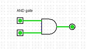
An AND gate is a logic gate that will only output TRUE if all inputs are TRUE. If this condition is not met, the output will be FALSE. In this image you can see an AND gate in its typical representation. It has two inputs (on the left) and one output (on the right). Please note that AND gates can have any number of inputs. It is not uncommon to see a 3-input AND gate.
The following save shows a functional AND gate (along with other gates) made in Powder Toy.
https://powdertoy.co.uk/Browse/View.html?ID=96171 (alexthesax)
OR gate
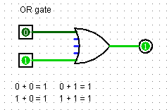
An OR gate is a logic gate that will output TRUE as long as at least one of the inputs are TRUE. An OR gate will also output TRUE if both inputs are TRUE. This is the typical representation of an OR gate.
(I would like to make a correction. 0 + 0 = 0. It does not equal 1. That was a typo on my behalf)
The following save shows a functional OR gate (along with other gates) made in Powder Toy.
https://powdertoy.co.uk/Browse/View.html?ID=96171 (alexthesax)
XOR gate
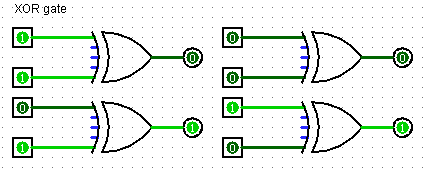
And XOR gate is slightly different to an OR gate. The X stands for exclusive. This means that the XOR gate will only output TRUE if one but not both inputs are TRUE. This is an example of an XOR gate in all of its states.
The following save shows a functional XOR gate (along with other gates) made in Powder Toy.
https://powdertoy.co.uk/Browse/View.html?ID=96171 (alexthesax)
NOT gate (or inverter)
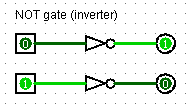
A NOT gate outputs the opposite of the input. For example, if the input was 1, the output would be 0. And vise versa. NOT gates are usually used in conjunction with AND/OR/XOR gates to reverse their functions. NOT gates are also used to represent the complement of a variable. For example if A = 1, then A' = 0. Placing a NOT gate after an AND gate (NAND gate) will represent this, and therefore, the output will always be the complement of A. This is the typical representation of the two possible states for a NOT gate.
The following save shows a functional NOT gate (along with other gates) made in Powder Toy.
https://powdertoy.co.uk/Browse/View.html?ID=96171 (alexthesax)
NAND/NOR/XNOR gates
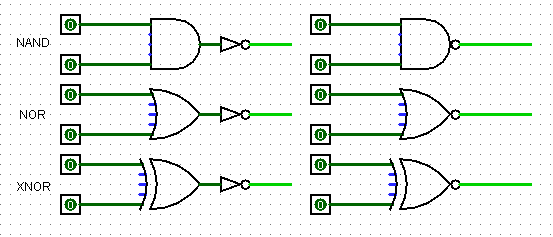
These gates are simply AND/OR/XOR gates with a NOT gate placed on their outputs. The resulting effect is that if the input was A + B =1(OR gate), it would change to A' + B' =1(NOR). If it was AB = 1 (AND gate) then it would change to A'B' = 1. If it was an XOR gate it would also invert. Note that XOR gates aren't represented in boolean algebra by the common addition or multiplication signs, however XOR is equal to AB' + A'B. This shows the three gates. I will show two ways to represent them (with a bubble on the outputs, and with the full NOT gate. Both mean the same thing).
Truth tables
Now that you have an understanding of the basic boolean algebra concepts as well as their logic gate equivalents, it is time to learn about truth tables. A truth table is a table used to show all of the possible outputs for a given set of inputs. It is also used to dictate the outputs a person would want from every possible combination of inputs. It is possibly the most powerful tool in creating a logic circuit that will do what you want it to do.
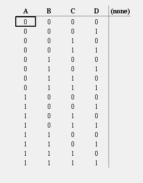
For example, what if we wanted to convert a 4-bit binary number into language readable by a 7-segment display. This means that we need 4 inputs for the binary number that we are attempting to convert. We will name these inputs A,B,C and D. Notice that the inputs were place on the left side of the table in columns. The (none) represents where we will place the outputs that have not yet been defined. As you can see the 4 inputs take up 16 rows in order to show every possible combination of inputs.
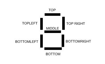
Next we will add the outputs. For a binary to 7-segment decoder we would need 7 outputs. 1 output for each segment of the display. Later we will link these outputs to 1 segment each. I labeled the outputs according to the segment they will be attached to (on the 7 segment display)
This shows the segments each output corresponds to.
Next we are going to assign values to each of the outputs. The way we do this is as follows.
1. We look at row one. The value in the inputs is 0 (A=0,B=0,C=0,D=0).
2. If the inputs were equal to zero, that would mean we would want to display zero on the seven segment display. So we change the value in each output column to 1, except for the value in the column labeled middle, because in representing a zero in a seven segment display, we would need to turn on every segment except for the middle one. If you correspond the values in this image to the image of the 7 segment digit, you will see that we have represented a zero. Assuming that the segments are lit up when a value of 1 is present and turned off when a value of 0 is present.
3. We will go down every row, one row at a time and do the exact same thing. Note that we will not need to continue after the tenth row, as for a single digit the highest value displayable is 9. (the values in the rows after A=1, B=0, C=0, D=1 (9) can be left as x, which means "don't care". By doing this we define that the outputs for the inputs 1001 to 1111 don't matter, and they can be either 1 or 0.) However if you were doing a hexadecimal display, you may want to use all of the rows. This is what your table should now look like (for 0-9).
Now we have finished our truth table. We have defined our inputs as A,B,C,D for our 4-bit binary input, and we have defined our outputs which each correspond to a segment on a seven segment display digit. The next step is to convert this table into a logic circuit.
Building the circuit
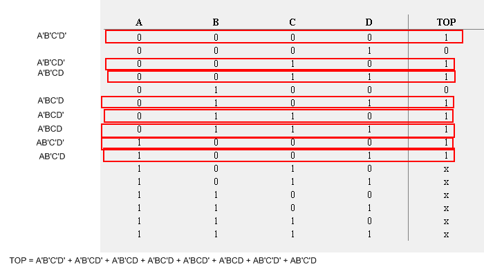
The next step is to extract the information from the truth table. To do this we will start by looking at each output. For the first output, TOP, if you look down its column you will notice that it is equal to 1 in 8 of the rows. Theses are the rows we are going to focus on.
Deriving the equations
We will focus on the TOP output for now. We are going to generate an equation from TOP. The method is as follows.
1. Look down the TOP column. As you can see, the first 1 is in row one. Take note of the value of the inputs in this row.
2. The inputs for this row are A=0,B=0,C=0 and D=0. Write on a piece of paper, TOP = A'B'C'D'
3. Once again look down the TOP column until you find the next 1. The next 1 is located on row three which has the values A=0,B=0,C=1 and D=0.
4. Add this to your equation like so. TOP = A'B'C'D' + A'B'CD (please note that a value of 0 is defined with the complementary sign, and a value of 1 is not. Also note that A'B'C'D is the same as A' * B' * C' * D'. * is the sign for multiplication.)
5. Now we are going to do the same thing for every other 1 found in the column and add them to the equation. It should look like so. With the finished equation for TOP.
6. The final step, is indeed going to be tedious, but you are going to have to do the same thing for every other output. Don't worry, I have to do it too, so it isn't that hard. Also note that usually it would be far quicker than this, but 7 outputs is a lot of outputs. After about 15 minutes this is the finished group of equations I came up with.
TOP = A'B'C'D' + A'B'CD' + A'B'CD + A'BC'D + A'BCD' + A'BCD + AB'C'D' + AB'C'D
TOPLEFT = A'B'C'D' + A'BC'D'+ A'BC'D + A'BCD' + AB'C'D' + AB'C'D
TOPRIGHT = A'B'C'D' + A'B'C'D + A'B'CD' + A'B'CD + A'BC'D' + A'BCD + AB'C'D' + AB'C'D
MIDDLE = A'B'CD' + A'B'CD + A'BC'D' + A'BC'D + A'BCD' + AB'C'D' + AB'C'D
BOTTOMLEFT = A'B'C'D' + A'B'CD' + A'BCD' + AB'C'D'
BOTTOMRIGHT = A'B'C'D' + A'B'C'D + A'B'CD + A'BC'D' + A'BC'D + A'BCD' + A'BCD + AB'C'D' + AB'C'D
BOTTOM = A'B'C'D' + A'B'CD' + A'B'CD + A'BC'D + A'BCD' + AB'C'D'+ AB'C'D
Building the circuit
Now we have the equations for each output. From this we can build a circuit. Please note that in the future I will be adding a section for simplifying these equations. As this is possibly the most raw unsimplified version possible, and will result in an extremely large and over-complicated logic circuit. But for now, I will just show you how this circuit is made. The method is as follows.
You can do this on paper, in Powder toy or in a program such as Logisim. I am going to be using Logisim, as it is the easiest to immediately layout and convey the method. Logisim is a free program and has an amazing feature which allows you to write a truth table, and it will automatically generate a logic ciruit for you, along with the equations.
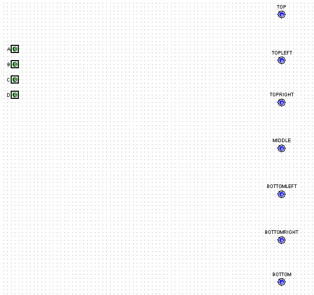
1. Layout your 4 inputs and 7 outputs in a similar way to this. Note that I am using Logisim for the sake of clarity.
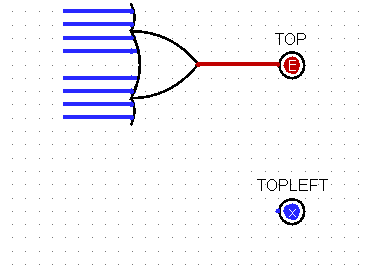
2. Lets look at the equations. Notice how they are all groups of inputs + groups of inputs. Remember that addition is the same function as an OR gate. We will look at the equation for TOP first. There are 8 seperate groups of 4 inputs.
The equation says TOP = A'B'C'D' + A'B'CD' + A'B'CD + A'BC'D + A'BCD' + A'BCD + AB'C'D' + AB'C'D. This means we need to use an OR gate with 8 inputs and 1 output. If you look at the equation you will notice that TOP does not equal A'B'C'D' * A'B'CD' * A'B'CD * A'BC'D * A'BCD' * A'BCD * AB'C'D' * AB'C'D. If this was TOP's equation, it would mean that TOP would only output TRUE if all 8 of those groups of conditions were met. However luckily the equation states differently. The addition signs in the equation means that TOP = A'B'C'D, TOP also = A'B'CD', TOP also = A'B'CD ect. So we can use an 8 input OR gate to show that all of these conditions don't need to be TRUE for the output to return TRUE, only one of them. So go ahead and place an 8 input OR gate where I have.
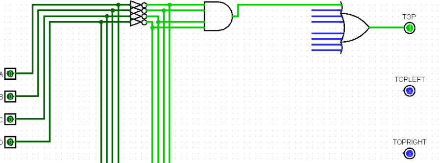
3. Continuing with the TOP output, the next thing we need to adress is the 8 groups of 4 variables. If you look at the diagram, you will see that every input to the OR gate actually corresponds to one of the 4 variable groups. For example, the up most input is supposed to be equal to A'B'C'D'. This group of 4 variables, along with all of the other variable groups, can also be represented as A' * B' * C' * D'. Remember that multiplication is the same as the function of an AND gate. So in order to make the uppermost input to the OR gate equal A'B'C'D', we are going to need to use a 4 input AND gate. The 4 inputs to this AND gate are must consist of the complement of A, the complement of B, the complement of C and the complement of D. How do we achieve this? With a NOT gate.
Let me explain what I have done. I first created a row of wires that travels vertically downwards. These rows represent the inputs A, B, C and D. I then branched each of these inputs off and used NOT gates to change their values to A', B', C' and D'. Notice how the second set of vertical wires is lit up. That is because they are the complement of whatever the input is, in this case the inputs are turned off, and therefore the inverted wires are equal to 1. I created an AND gate and I linked A',B',C' and D' to its inputs. I then linked the output from that AND gate to the top most input for the OR gate.
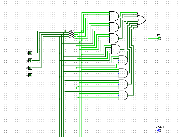
4. The next step is to do the same thing for the other 7 groups. This is what it should look like after you have finished. (Remember that is an extremely unsimplified version, and later on I will a section on karnaugh maps and equation simplification, which will give you a far smaller circuit.
5. Now you need to do the exact same thing you did in steps 2,3 and 4 for every other output. This is what it should look like (this has been completely re-arranged in order to create more space. It will look different, but it won't matter because creating the circuitry for the other 6 outputs is exactly the same method as used for the first output.
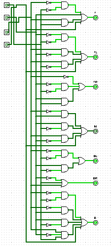
This is the finished result after re-arranging. I got rid of the row of complemented inputs and just placed NOT gates where needed to conserve space. The image is so damn long that I had to use another method to save it, which doesn't have colour. I will make a new one soon. Please note that on this image the "1" on the outputs doesn't mean that the output is TRUE. It just seems to be there regardless. In actuality every output is TRUE except for the middle output which is FALSE. This represents zero on a seven segment digit. Although it doesn't show this on the image, where it says every output is 1/TRUE.
Simplification with karnaugh maps
In this section I will show users how to simplify their circuits with algebraic simplification and karnaugh maps. This is an example of how far the binary to 7 segment decoder can be simplified.
Introduction to karnaugh maps
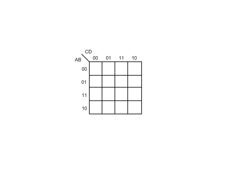
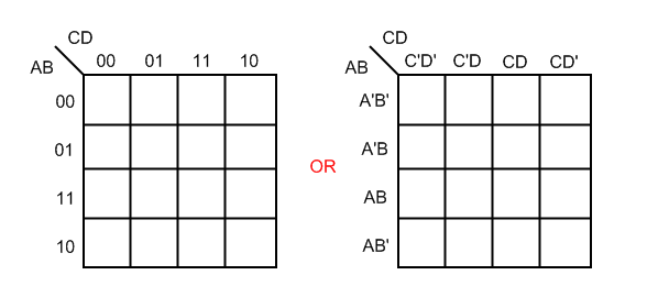
Karnaugh maps are useful instruments in simplifying your logic circuits. These maps come in various sizes depending on the amount of inputs your circuit has. Our circuit has 4 inputs (ABCD) so we will be using one of these karnaugh maps.
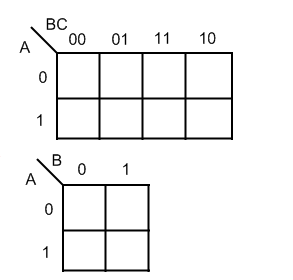
Here are some other example sizes. For three inputs and two inputs.
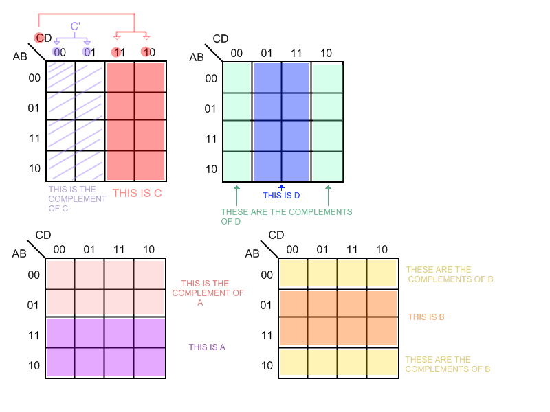
Karnaugh maps are similar to venn diagrams, if you have ever used one. The box as a whole represents every input and its complement. Each input has its own area in the map, and each complement of those variables also has a region. This shows what I mean by that.
If you look closely at the image you will notice that 0 is used to represent one of the inputs complements, and 1 is used to represent the inputs actual designated area. Anything residing inside of a certain inputs area is said to belong to that input. Whereas anything residing in a certain inputs complement, belongs to that complement. However since this is a grid and a single square on the grid cannot be located and defined just by one input (just as you cannot pinpoint a point on a grid with only x and not y) we will need to used several inputs in order to define it. First of all, this image illustrates another way you can make your karnaugh graph, by replacing the 0 and 1's with their respective input values for example A'B. This will make it easier for many people to actually identify points on the map.
Using the karnaugh map
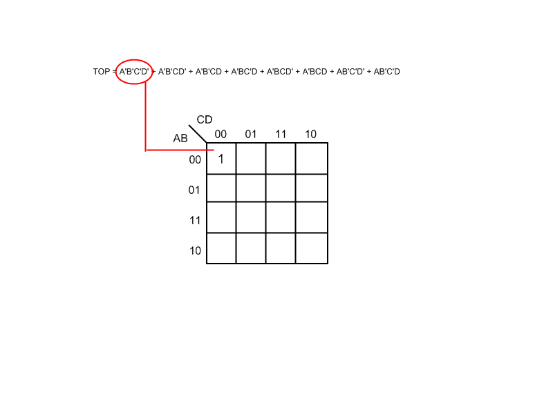
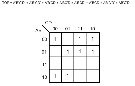
In order to use the karnaugh map, we are going to have to look at each output (TOP, TOP LEFT ect) separately and plot the equation for each onto the graph. We will start with TOP. The first thing we need to do with TOP is to look at the first part of its equation which is A'B'C'D'. This is a very easy point to plot. To make it easier to plot this point, I am going to show you a trick. If you look at the group, they are all complements. If we assign complements 0 and non complements a 1, then we can convert it into a string of numbers. This is 0000. Now look at the graph, starting on the west side. Look for 00. When you find 00 you will need to go to the north side of the map and look for 00 again. After you have done that, just mark the intersection between 00 and 00 by writing a (1) in that square.
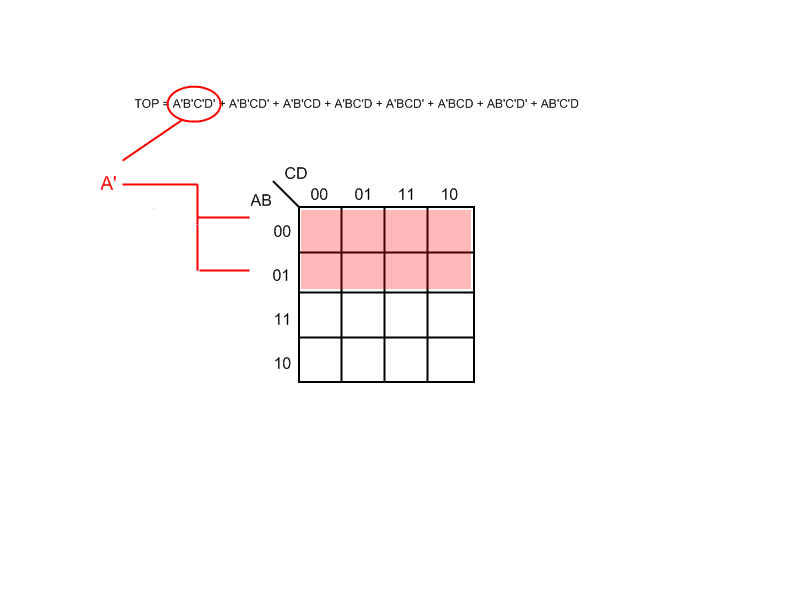
Here is a different approach, and if you are confused, maybe it will shed some light on things.
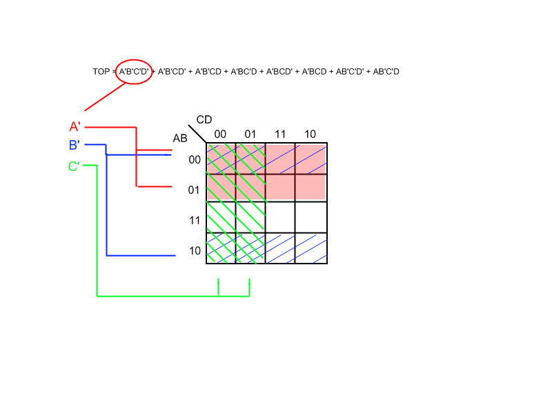
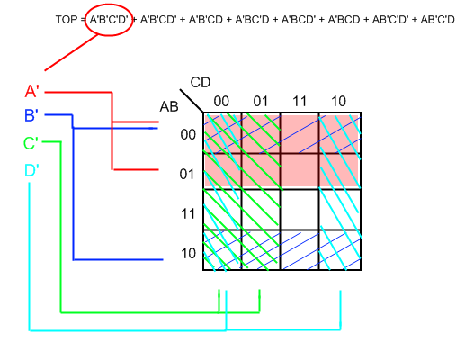
First off you need to find A'. A' consists of two rows. I shaded the region with a light red to illustrate.
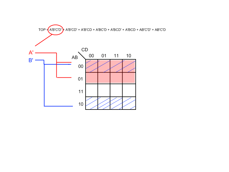
Now we will look for B'. I covered the region with blue diagonal lines to show this.
Now let's find C'. I covered the region with green diagonal lines to show this.
Now finally we will find D'. D' is shown by the teal diagonal lines.
As you can see, there is only one square in the entire map that has been shaded by all four inputs. And this is the top left square (0000). Place a 1 there if you haven't already. The next thing to do is to do the same for the other seven parts of the equation. When you have finished it should look something like this.
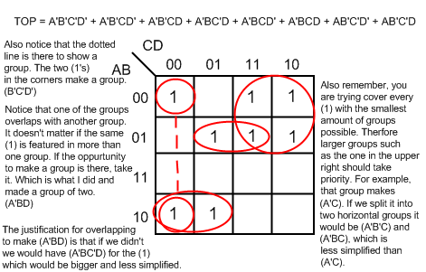
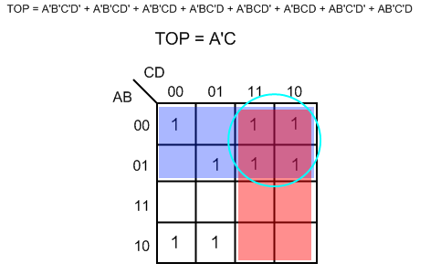
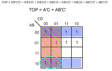
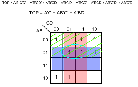
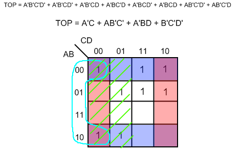
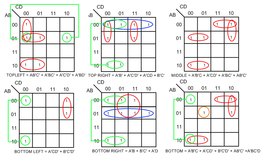
The next step is slightly more difficult. In order to simplify the equation we are going to need to group the points in a way that allows us to read them off the graph again, but this time with a smaller equation. Groups can be formed by (1's) that are next to each other, by (1's) that create squares, (1's) that cover a whole row or by (1's) that share a common input. It is a hard concept to grasp initially, but I will be showing an example for every inputs equation (TOP, TOP LEFT, TOP RIGHT, MIDDLE, BOTTOM LEFT, BOTTOM RIGHT, BOTTOM). It is really important to note that you cannot form a group that doesn't fill in an entire area (say A) and define that group by A. For you to define a group as A and only A, that group would have to fill in the entire two rows that A represents. This is why we are often left to define a group by using more inputs. Look at this image. It shows the way I have grouped each 1. There are two things about this image to note. Firstly that groups can overlap, and if you are given the choice of leaving a point singular, or overlapping it with some other group, you should choose the latter. Because it is always beneficial. Secondly, larger groups are better. The more points (1's) that you can define by using a single group, the better.
Here are the steps I took to finding these groups and writing down the new equation.
1. I decided I wanted to make a group from the square. It is a large group and allow for a large amount of simplification. I shaded the two areas that create the coordinates I need to define the group. I wrote the coordinates above the map in the new equation.
2. I grouped the two (1's) in the corner. This group needs three variables to be defined, not just two. Hence, larger groups are better because they define more (1's) with less variables. Notice that the group takes up the entire area of (AB'C')
- I apologize, I actually shaded this image incorrectly. Instead of shading A, I shaded C' twice. If you picked up on this then you are doing well. But just imagine that the area of A was shaded.*
3. I chose to form a group by using the 1 that was next to the square group made in the first step, and I used a 1 from the square that was defined earlier. Overlapping like this is a good thing, and it doesn't matter how many times you define the same point.
4. This one is interesting. You may not think this as a group, but it is. They both belong to B'. I also intersected with the group made in step 2.
Now that we have finished defining the new simplified equation for this input (TOP), we are going to do the same thing for every other input. Here is an image showing the grouping and new equations I made for every other input. Notice how much smaller the equation for BOTTOM RIGHT has been made. It previously contained 36 variables (4 * 9), now it only has 6.
For convenience, here are the new equations.
TOP: A'C + AB'C' + A'BD + A'B'C'D'
TOPLEFT: AB'C' + A'BC' + A'C'D' + A'BD'
TOPRIGHT: A'B' + A'C'D' + A'CD + B'C'
MIDDLE: A'B'C + A'CD' A'BC' + AB'C'
BOTTOMLEFT: A'CD' + B'C'D'
BOTTOM RIGHT: A'B + B'C' + A'D
BOTTOM: A'B'C + A'CD' + B'C'D' + AB'C' + A'BC'D
And the new logic circuit we can derive from this. (65% smaller than the original)
Let your pc do the dirty work
This Windows program solves Karnaugh maps for you. Conveniently placed after the tutorial :D (you probably hate me for that, but it's always better to know how things work first)
Powder toy adaptation (whole section coming soon)
This section will eventually contain more images that make it easier to follow on powder toy, but for now I will just show a powder toy version of the logic circuit we just made. Notice it is arranged slightly different (I made a separate set of rows for the NOT gates).
https://powdertoy.co.uk/Browse/View.html?ID=536556
--Jayden Traynor 09:35, 7 October 2011 (BST) (synergy)
